But wait a
minute. Didn’t we read something about the Tegra K1 being a 192-core chip?
Well, what NVIDIA is referring to is the mobile Kepler GPU that will be in both
the 32 and 64-bit versions of the K1, which is the other big thing in this K1
story. For the uninitiated, these 192 CUDA cores are based on NVIDIA’s desktop
Kepler GPU architecture, the same one used in the GeForce 600 and 700 series of
desktop GPUs. But compared to desktop Kepler, this mobile Kepler is a mere 2W
GPU.

NVIDIA
Tegra K1 reference design tablet hands-on
The other
huge benefit of implementing the same GPU architecture across both desktop and
mobile platforms is that both get the same level of API support, thus making
life so much easier for developers to port their desktop and console engines to
mobile devices like smartphones and tablets. The Tegra K1 supports OpenGL ES
3.0, OpenGL 4.4, DirectX 11, tessellation, and CUDA 6.0, and it’s also the
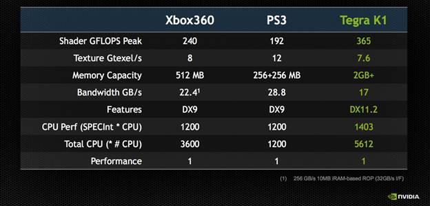
first mobile GPU to support the Unreal Engine 4 game engine. For those lost in
all these geek speak, just know that the K1’s graphics prowess supposedly
betters that of the PlayStation 3 or Xbox 360. We’ve heard of ‘console-level
graphics’ being thrown around a lot by mobile chipset makers, but looks like
this time it’s for real. And we’re pretty sure NVIDIA has approached Microsoft
and Sony, who besides making the PlayStation and Xbox, are also making phones
and tablets.

First
Class Gaming Flatform
Several Questions Unanswered
At this early
stage, the Tegra K1 looks super promising. Tom’s Hardware has some 3DMark
results that show the 32-bit, quad-core K1 outperforming the Qualcomm
Snapdragon 800 and the Apple A7. And in the GFXBench graphics benchmark, the K1
also outruns Qualcomm and Apple’s chips, offering nearly double the frame rate
at 1080p. Of course, one should take these results with a pinch of salt,
because the K1 used here was in a Lenovo ThinkVision 28, a huge all-in-one
desktop device. In other words, the differences in power management and cooling
options may have skewed the results.

The quad-core
K1 outperforming the Qualcomm Snapdragon 800 and the Apple A7 in 3DMark
Also at this
point in time, there are still several unanswered questions regarding NVIDIA’s
‘super chip’. While both versions of the Tegra K1 are likely to be fabricated
using TSMC’s 28nm HPM process, judging from NVIDIA’s presentation slides, if
drawn to scale, a Denver core is twice as big as a Cortex-A15 core. No die size
details were given, so the K1 may well turn out to be a big chip. And while
NVIDIA may have successfully built a low-power mobile Kepler GPU, the power
consumption of the whole Tegra K1 package is still an unknown. Lastly, it remains
to be seen if NVIDIA can ship the K1 on time, especially the Denver-based K1,
which is expected to arrive in the second half of this year.
As things
stand now, it looks increasingly likely that the majority of the SoC battles
come late 2014 and early 2015 would be fought on the GPU front.