The Inaugural Maxwell Card - NVIDIA GTX 750
Ti (Part 1)
A Portent Of Things To Come…
Well, this is a first. Here we are with a
brand new GPU architecture from NVIDIA and for once it’s not debuting in some
flashy $830 top-end graphics card. Instead, NVIDIA has decided to introduce the
new Maxwell design in a mainstream graphics card, the GTX 750 Ti, right from
the off.

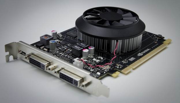
NVIDIA has taken the wraps off the GTX
750 Ti
That’s why there’s been no bombastic
launch here, no lengthy deep dive sessions in some dusty conference room, and
barely a whimper from the engineers involved. NVIDIA is essentially testing the
Maxwell waters.
NVIDIA is calling this GTX 750 Ti
Maxwell’s first generation of GPUs, but in these days of Early access it feels
almost like a beta release of a graphics architecture. That may sound a little
unfair – this isn’t some half-baked release or a buggy silicon setup. We’re
only phrasing it in such language to indicate that this is a very different
architecture debut to those we’ve previously seen from the mean green machine.

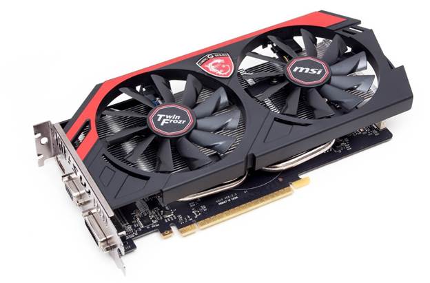
This is a GeForce GTX 750 Ti overclocked
properly
It’s actually rather smart of NVIDIA to
roll out Maxwell in this way, especially if you take a look at NVIDIA passim.
Historically, things haven’t gone particularly well when it rolled out a new
graphics architecture at the same time as a drop in the production process.
We’re looking at you, Fermi… When the GTX 480 was first introduced on the 40nm
process, the yields weren’t great; the chip came out frighteningly hot and
power-hungry. It wasn’t really until the GTX 580 update that the Fermi
architecture actually matured.
Keeping the new GTX 750 Ti and its Maxwell
architecture on the same 28nm lithography as the previous generation means that
NVIDIA has been able to iron out architectural bugs without having to worry
about unforeseen process problems, and since 28nm yields are as good as they’re
likely to get, it makes perfect sense for a mainstream, high-volume card to
roll out on a process that’s going to be produced in numbers.

The new GTX 750 Ti on the same 28nm
lithography as the previous generation
It’s almost aping Intel’s method of CPU production
– its tick-tock cycle. Intel creates a new architecture on an existing
production process and then refines the same architecture with a die shrink –
the tick being the shrink and the tock being the new microarchitecture. This
could just be a happy accident of circumstance. As far as we know, Maxwell had
initially been penned in for the 20nm process, but TSMC has had some problems
with new technology shrinks stretching back to the 40nm to 32nm drop. That node
was eventually cancelled and it went directly to 28nm – where it has managed
impressive yields – with the 20nm process not likely to enter into mass
production until the first quarter of this year.
Without NVIDIA knowing for sure when it
would be able to get significant volume on a new lithography, it had no choice
but to release its new architecture on an existing production process.