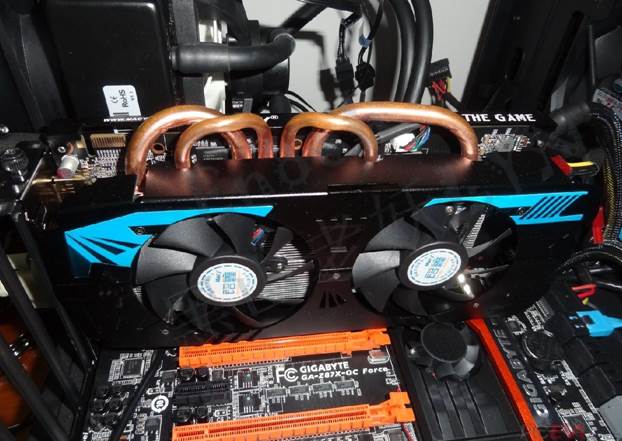
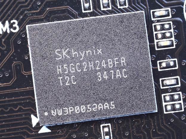
The Inaugural Maxwell Card - NVIDIA GTX 750
Ti (Part 2)
A Portent Of Things To Come…

The GeForce GTX 750 Ti GPU would feature
a revised
GK106 core equipped with 960 Cores, 32 ROP and 80 TMUs
Ultra efficient
Enough of the whys, though. What is
Maxwell all about? In a word: efficiency. That’s been the buzzword around
pretty much all of our technology in recent years, but it has taken GPUs a long
while to catch up. The graphics card is most likely the hottest and loudest
part of your Pc, and that’s partly because we’ve allowed it to be. We want the
fastest, smoothest frame rates in our games and we’ll happily sit on a turbine
to get there.
But the times, they are a-changin’.
Whereas once you could rely on a new die-shrink to offer the chance to get more
processor logic into the same space at an equal cost or less, the technological
demands of ever-shrinking transistors is rising more and more with each shrink
in process – and that rising cost of development comes hand in hand with
production cost increases. In order to get more with less, as much performance
per watt as is technologically possible must be developed. And that’s Maxwell’s
raison d’être.

It’s now time for Nvidia to launch their
latest and greatest GPU – Maxwell
The upshot of this is that graphics cards
will get more efficient in terms of power demands and temperatures. The first
seeds have been sown with the advent of this 28nm first generation Maxwell GPU
and will only improve with the move to 20nm.
More performance
In terms of the architecture, Maxwell
inevitably shares DNA with Kepler and Fermi, being made up of many little CUDA
cores for that parallel processing goodness we know and love. It’s the
management and arrangement that’s different. The big change is in the streaming
microprocessor. The SM has evolved from its first appearance with the Fermi
architecture: it was redesigned as SMX for Kepler and now as SMM with Maxwell.
The new SMM re-organises the control logic
and the CUDA cores themselves. With the previous design, each SMX housed 192
CUDA cores that were looked after by a single piece of control logic. With
Maxwell, every SMM is divided into four quadrants, with 32 CUDA cores in each,
and each with its own control logic. That does mean there are now only 128
cores in every SMM, but each of the four processing blocks has its own
instruction buffer and scheduler to improve efficiency and overall processing
speed.

There are now only 128 cores in every SMM
The SMMs are now smaller, which means that
NVIDIA has been able to squeeze five of them into this GM107 GPU. This added
logic and higher number of streaming microprocessors – analogous to what AMD is
now referring to as compute cores – Adds to the parallel processing power of
the Maxwell chips and, according to NVIDIA’s testing, means it can deliver
around 35 percent more performance from each CUDA core.
That’s why this GTX 750 Ti is able to sit
alongside the likes of the GTX 650 Ti Boost in terms of performance, despite
being much lower-powered and having fewer CUDA cores housed within. The GM107
GPU is the inaugural Maxwell GPU, and the GTX 750 ti represents the chip at its
full implementation. There is also a GTX 750, which is running the same GM107
GPU but with one less SMM and half the video memory.