The wrapper of HIS
7950 IceQ X² Boost Clock 3GB is designed in the same style as its senior
version’s, except the product’s name and the lack of the advantage of the
cooling system.

There is a Boost
Clock badge in the middle of the box, but its information does not match with
our testing data as well as that on the official website.
Wrapper,
accessories, manufactured country and warranty are the same as HIS 7970 IceQ X2
GHz Edition, but HIS 7950 IceQ X² Boost Clock offer a less expensive price of
$319.
HIS 7950 IceQ X²
Boost Clock is the visual difference with its senior relatives, which have the
same size, video interface and cooling system.

The cooling system

HIS
7950 IceQ X² Boost Clock
The only difference that could be found is
the 6-pin and 8-pin connections instead of two 8-pin connections.
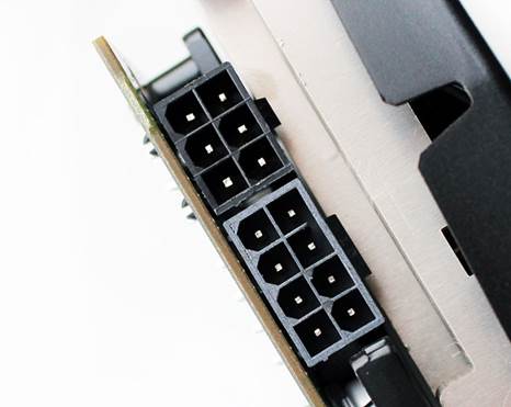
6-pin
and 8-pin connections
We can remind you that the reference Radeon
HD 7950 has two 6-pin power connections. HIS version has the same power
requirement as the reference card: consume maximally 200W and a PSU 500W or
better.
HIS 7950 IceQ X² Boost Clock takes after
HIS 7970 IceQ X² GHz Edition in its PCB design, except some specific elements
which are not easy to recognize.
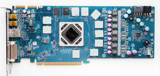
PCB
design
The card seems to be used with the
DirectFETs, with the solid capacitors and 6+1+1 phase power system and a CHiL
CHL8228G controller.
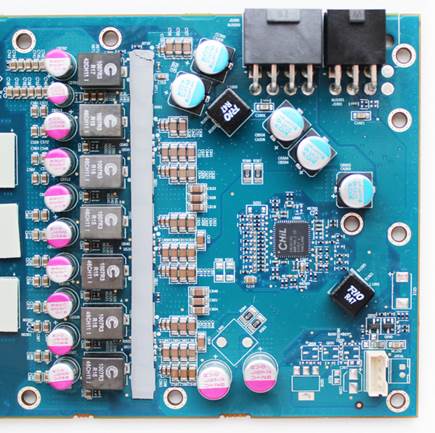
DirectFETs,
solid capacitors
The website of the producer say about a
4+1+1 (CPU + memory + PLL) which we tend not to agree about.
There is no unusual sign of Tahiti Pro chip
in HIS 7950 IceQ X² Boost Clock. Its sign can be read on GPU’s metallic frame.
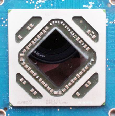
Tahiti
Pro chip
GPU clock rate is 850MHz but we have never
recognized this rate in our tests. It has always been 950MHz (The so-called
boost mode, therefore card’s specified Boost Clock). By the way, that is such
an impressive overclock. The voltage is 1.25V in 3D mode and 0.806V in 2D mode.
The GPU is clocked at 300MHz in 2D applications.
The card is equipped with a 3GB GDDr5
memory in 12 Elpida memory chip on the surface of the PCB.

12
Elpida memory chip
Based on our experience, we chose Hynix to
Elpida when considering about overclock potential. HIS has to attempt to reduce
its expenditure by installing cheaper variants. Labeled W2032BBBG-50-F, the
memory chips are estimated 5000MHz. We really did clock at that frequency,
providing the maximum bandwidth of 240GB/s via a 384-bit bus.
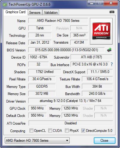
The
maximum bandwidth of 240 GB/s through a 384-bit bus
HIS 7950 IceQ X² Boost Clock owns the cooling
system like the premium HD 7970:
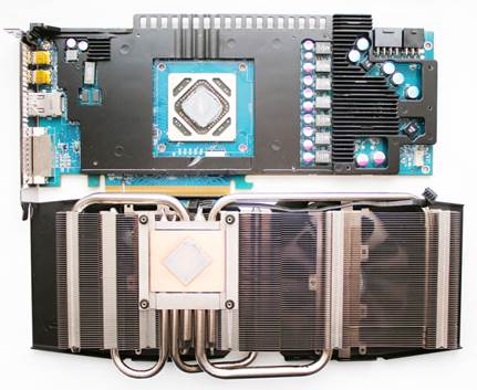
The
cooler of HIS 7950 IceQ X² Boost Clock
We again describe, so let’s move to the
part of checking its performance. First, let’s start with the default
interface.
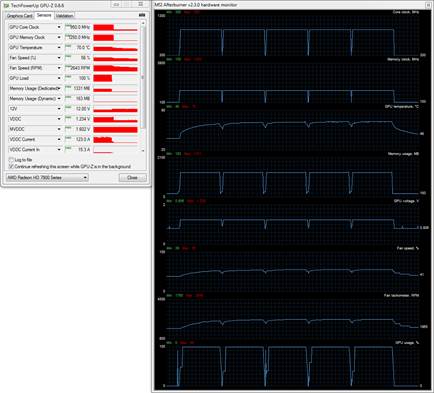
The
auto fan mode

The
maximum fan speed
Because IceQ X2 works well on
high-speed Radeon HD 7970, it should not have any problem with HD 7950. In
fact, the GPU is 70°C hot in auto fan mode (2640RPM) and 66°C in the maximum
fan speed mode (3880RPM)
The temperature is 4 to 5°C lower in each
mode after replacing the default thermal interface with ARCTIC MX-4.
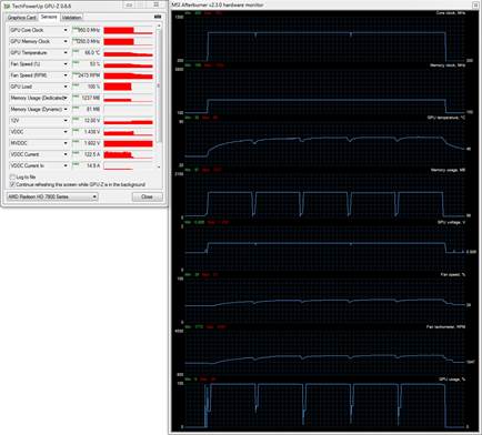
The
auto fan mode

The
maximum fan speed mode
We could also add something to this that
the fan speed increased from 2640 to 2470RPM in the auto fan mode, so we made
quite little noise. The practical benefits of replacing the default thermal
interface are obvious.
However, we checked the overclock ability
of the card with its default interface. The GPU clock rate could be increased
from 950 to 1140 MHz, about 34.1% higher than the GPU frequency of the
reference AMD Radeon HD 7950. However, the memory chips were disappointing that
they were just 5960MHz.

GPU
clock rate can be increased from 950 to 1140MHz
Thus, the result of HIS 7950 IceQ X² Boost
Clock clock rate is 1140/5960 MHz
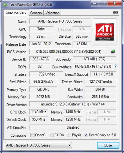
HIS
7950 IceQ X² Boost Clock clock rate is 1140/5960 MHz
Just like HIS 7970 IceQ X² GHz Edition, the
GPU’s peek thermal increases 3°C at 2830 RPM at the overclocking frequencies.

The
GPU’s peek thermal increases 3°C
|
Specifications
·
Graphic processor: “Tahiti Pro” (TSMC)
·
Production process: 28nm (low-k)
·
Mold size: 365mm2
·
Transistor: 4314mln
·
GPU frequency: 3D (850 – 950 (boost) MHz), 2D
(300MHz)
·
GPU voltage: 1.25V (3D), 0.806V (2D)
·
Unified shader processor: 1792
·
Texturing unit: 112
·
Rasterization: 32 (ROPs)
·
The maximum theoretical filling rate: 30.4
(Gpixel/s)
·
Texture rate: 106.4 (Gtexel/s)
·
Pixel shader/ Peek shader: 5.0/5.0
·
Supportive memory type: GDDR5
·
Frequency of video memory: 5000MHz (3D),
600MHz (2D)
·
Memory capacity: 3072MB
·
Momery bus: 384 bit
·
Memory bandwidth: 240.0 GB/s
·
Maximum power comsumption: 200W (3D), 70/3W
(2D)
·
PSU requirement: 500W
·
Reference PCB size (D x R x S): 311x150x42 mm
·
Interface: PCI- Express x 16 (v3.0)
·
Output: 1DVI (Dual-link), 1 HDMI, 2
DisplayPort mini
·
Retail price: $319
|