The flagship graphics accelerator of
Nvidia's new product line was introduced quite surprisingly. It not only
increases the performance bar but also the price maximum. Our review today will
reveal how such a large increase can occur on every aspect.
The preparation for the launch of Nvidia's
flagship graphics card have been pretty fast, ignore a couple of months of
rumors, information leakage and discussion of different versions of
specifications. Contrary to some skeptical predictions skeptical, Nvidia has
successfully introduced its top solution very quickly, and largely because the
company has recently released the special GeForce GTX Titan. The GeForce GTX
780 is based only on the Titan's design and uses the same GK110 GPU.

GeForce
GTX 780 graphics card
Why would we call the GeForce GTX 780 a
flagship product if we knew that the Titan was even faster. In fact, the Titan
is an image-constructive product and has very small target customer. As for the
GeForce GTX 780, it is a fast but standard graphics card. As the name implies,
it is meant to lead the top new product line of Nvidia. There is also one more
reason to call the GTX 780 a flagship product, but we will explain it in the
contents of this review.
Structure
The Nvidia GeForce GTX 780 is based on the
same GPU with the Titan: GK110 chip with Kepler structure. A SMX sub-unit is
turned off, however, in its GPU, so the total number of CUDA cores is reduced
from 2688 to 2304 or 14%.

A
SMX sub-unit is turned off
The number of texture-mapping units (TMUs)
was reduced from 224 to 192 but the number of raster operators remained at 48.
The GPU operates at higher clock rate: 863 MHz in 3D applications (up to 902
MHz in enhanced mode). Memory clock rate remained at 6008 MHz, but the new card
has 3 instead of 6 gigabytes, which affects the price and PCB design. On the
other hand the GeForce GTX 780 has the same power requirement as the Titan: 250
watts at maximum load. A 600 watt PSU source is recommended for a PC with a GTX
780 card inside.
Its introductory price is $649, which was
higher than 30% when compared to the GeForce GTX 680 ($499 - but the actual
retail price is now lower) and lower than 35% compared to the Titan.
Graphics card's design and features
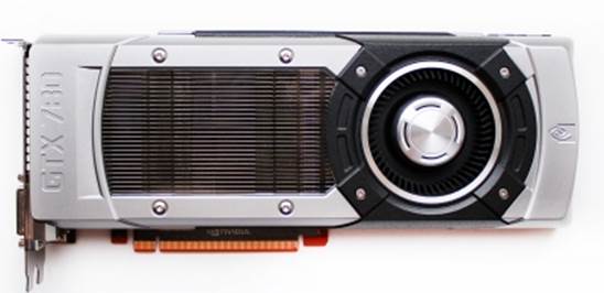
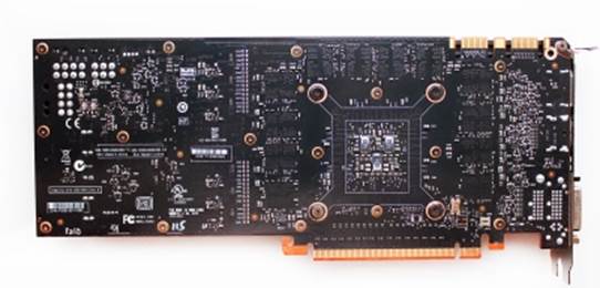
The new GeForce GTX 780 looks like a clone
of the GeForce GTX Titan except for the text on the cooler casing and the lack
of memory chips on the reverse side of the PCB.

The
GeForce GTX 780's front

The
GeForce GTX 780's rear
You will be pleased to know that the
GeForce GTX 780 has the same highlighting on its top edge as the Titan.

The
highlighting on the edge of the card
The new Graphics Card is equipped with
three video ports: dual-link DVI-I and DVI-D, HDMI 1.4a and DisplayPort1.2

The
ports of GeForce GTX 780
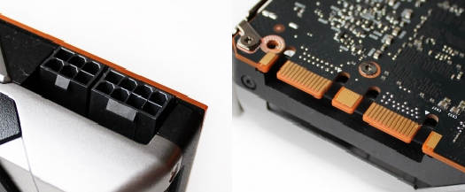
So you can connect multiple monitors at the
same time with a GTX 780 card just like with the Titan. There is no difference
in terms of power and SLI connector.

Power
and a corner of the GeForce GTX 780
PCB of previous versions of the GeForce GTX
780 is a copy of the Titan's PCB.

Being
a clone of Titan's PCB
Except for the change in the back of the
PCB that has been previously mentioned, the rest are the same. The GPU's
regulators consist of 6 phases of GPU-based DrMOS semiconductor, and three more
phases for the chip memory and PLL.

The
GPU's regulators consist of 6 phases of GPU-based DrMOS semiconductor
Like the Titan, the power system is
controlled by the NCP4206 controller of Semiconductor ON.

The
NCP4206 controller of Semiconductor ON.
Maybe the pre-installed GeForce GTX 780
will have another PCB.
The GPU of our samples are produced in
Taiwan in the 36th week of 2012. Thus, Nvidia had working GK110 chips as far
back as the early September 2012.

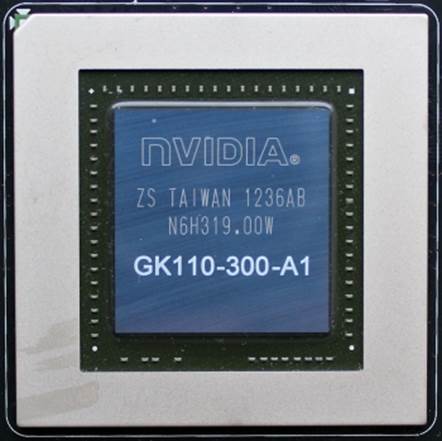
The
GPU die is 561 sq. mm large and marked as GK110-300-A1
The GPU die is 561 sq. mm large and marked
as GK110-300-A1 (the Titan die is marked as GK-110-400-A1). As specified in an
official way, the GPU is clocked at 867/902 MHz in 3D applications at 1162
volts. The clock rate was reduced from 324 MHz in 2D applications and the
voltage dropped to 0.875 volts.