Formerly called HSI (High Speed
Interconnect) and later 3GIO (3rd Generation I/O), PCI Express came into
existence in 2003, the same year as the SATA interface, coincidentally. The
protocol it replaced, PCI, used a parallel bus interface in which every device
(up to a maximum of five devices) connected to the PCI host shared the same
address, data, and control lines, which restricted communications to a single master
at a time and in just one direction.

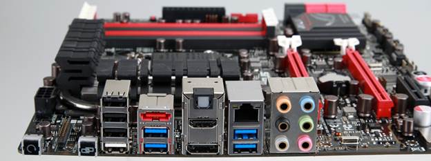
PCI-Express
support includes two 16x lanes that work 16x/1x or 8x/8x, along with
an open-ended 4x underneath and a 1x mPCIe via the Combo card
Clock rates on PCI were also reduced to the
speed of the slowest component connected, and electromagnetic interference
between the wires had become increasingly cost-prohibitive to prevent. PCI
Express dumped the parallel bus and relied on an interface that essentially
serialized the serial interface. PCI-E is a point-to-point serial interface
that supports dedicated links between each component and the PCI-E hub; it lets
full-duplex communication take place between the hub and component. As such,
multiple PCI-E devices can communicate with the hub simultaneously without
suffering a delay or taking a bandwidth hit from a slower-performing component.
Traditionally, each link extending from the
PCI-E hub corresponds to a physical slot, but the slots come in different form
factors that support different numbers of lanes (each of which consists of two
differential signaling pairs, one for sending data and the other for receiving).
The slot attached to a single-lane PCI-E interface is called a PCI-E x1 (by
one) slot, and it sends one bit per clock cycle. The x4, x8, and x16 slots each
transmit four, eight, and 16 bits per clock cycle, respectively.

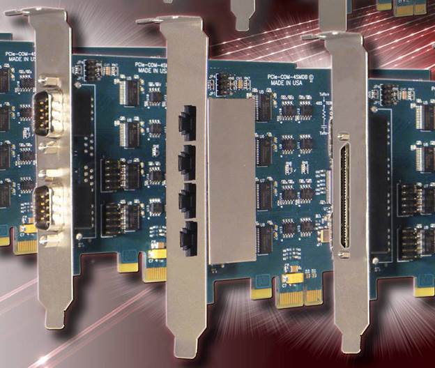
PCIe-COM
series feature selection of 8, 4, or 2 ports of
software-selectable RS-232, RS-422, and RS-485 serial protocols.
Each PCI-E lane has the bandwidth to handle
bidirectional 250MBps transfer rates. Four years after PCI-E’s debut, the 2.0
revision effectively doubled the data rate for each PCI-E lane—500MBps in each
direction. The latest version, PCI-E 3.0, alters the encoding scheme to
dramatically reduce the overhead required to shift packets between the PCI-E
hub and the individual devices. Where PCI-E 2.0 transmissions could have up to
20% of their total throughput set aside for overhead, PCI-E 3.0’s overhead
costs are closer to 1.5% of the total available throughput. The more efficient
encoding scheme translates to a real-world performance boost, delivering a
per-lane 985MBps data rate. Based on these numbers, you can see how the SATA
protocol could realize significant performance improvements by tapping into the
latest PCI-E revisions.
Big B Or Little B?
Before we delve into SATA’s transformation,
you may have noticed that we aren’t using bits per second to express speeds.
Although they both utilize serial data links, SATA and PCI-E encode data
differently, making it difficult to compare data rates using Mbps/Gbps. This is
because SATA’s 8b/10b (10-bit symbols used to encode 8-bit words) encoding
scheme lets the 6Gbps data rate translate to a 0.6GBps data rate. PCI-E 3.0, on
the other hand, uses a 128b/130b (130-bit symbols used to encode 128-bit words)
encoding scheme, which lets the protocol achieve a far more efficient 8Gbps per
lane to nearly 1GBps per lane data rate translation.

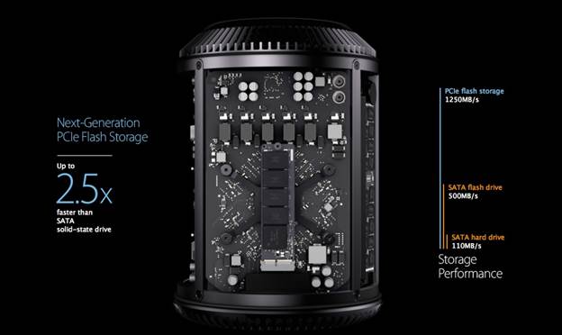
The
system will use the next-generation PCI Express flash storage technology
Both PCI-E 2.0 and 1.0 rely on the same
8b/10b encoding scheme as SATA, and as a result the peak 2.5Gbps and 5Gbps per
lane data rates for those protocols translates to 0.25GBps and 0.5GBps per
lane, respectively. In this way, a single lane of PCI-E 3.0 has an approximate
67% advantage in GBps over SATA III. And the new SATA 3.2 revision supports
even more than that.