The third constituent component of the
Trinity is the integrated North Bridge responsible for system memory access.
The Socket FM2 platform specially developed by AMD for the new APU generation
supports dual-channel DDR3 SDRAM at frequencies up to DDR3-1866. Because both
CPU and GPU cores used this memory controller, the memory bandwidth becomes a
critical factor. However, to reduce the transistor budget and lower the
manufacturing cost, the Trinity is devoid of L3 cache memory which would be
most useful in this design.
The Trinity series includes several APU
modifications varying not only in clock rates of their x86 and graphics parts
but also in the number of CPU cores and GPU stream processors.
Note that, although the Trinity used a
graphics core with VLIW4 rather than GCN architecture, AMD markets it as Radeon
HD 7000 because the Devastator is compatible with DirectX 11, OpenGL 4.1 and
OpenCL 1.1 APIs and features AMD’s latest video engine HD Media Accelerator.
Thus, the Trinity offers the ability to handle large HD video solution that
including hardware decoding of popular formats (UVD3) and hardware encoding
into H.264 format (VCE).
Now let’s have a closer look at the APUs
we’re going to test.
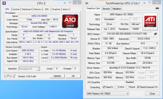
AMD
A10-5800K
A10-5800K is the top model of the Trinity
series. AMD uses it to showcase the benefits of the company’s new design, so it
has the maximum number of execution cores and shader processors and runs at
highest clock rates. As a result, we have a quad-core APU based on two
Piledriver modules with a base clock rate of 3.8 GHz and capable of
turbo-boosting to 4.2 GHz. Its integrated Radeon HD 7660D graphics core has
384 shader processors and is clocked at 800 MHz.
AMD
A10-5800K
With Turbo Core technology enabled, the APU
spends most of its time at 4.0 GHz, dropping the clock rate to 1.4 GHz when
idle. The clock rate is also reduced at high multithreaded loads: to 3.4 GHz
rather than to 3.8 GHz as you might have expected from the specifications. It
seems like the manufacturer announced an overstated base clock rate, and the
rather high TDP of this model, 100W, doesn’t make the A10-5800K any more
attractive.
Generally, the A10-5800K seems to be an
APU for overclocking and benchmarking experiments rather than for everyday use,
especially as it comes with unlocked frequency multipliers. You can easily
increase the clock rate of its execution and graphics cores and of system
memory above default levels.
A10-5800K’s specs
·
Number of cores: 4
·
CPU frequency: 3.8GHz Base, 4.2GHz Turbo
·
L2 cache: 4MB
·
Integrated graphics: HD7660D
·
Shader cores: 384
·
GPU frequency: 800MHz
·
TDP: 100W
·
Maximum memory frequency: DDR3-1866
AMD A10-5700K
The A10-5700 is the senior “normal” version
of the Trinity. Its TDP is limited to a modest 65W, making it suitable for
compact and energy-efficient computers. Although AMD have to significantly
reduce the clock rate to activate it The A10-5700 works at 3.4 GHz by default
and the clock rate grows no higher than 4.0 GHz in the turbo mode. The clock
rate of Radeon HD 7660D graphics core is also reduce to 760 MHz. With all these
limitations, A10-5700 is a fully functional Trinity with with all x86 cores and
shader processors active. The lack of L3 cache is pretty disappointing, but
that is a prominent feature of the whole Trinity design. Each dual-core
Piledriver module in the senior Trinity APUs has a dedicated 2MB L2 cache, so
we have a total of 4 MB of L2 cache for the entire chip. it is only connected
to the x86 cores and doesn’t help the graphics core or in processing shared
data of heterogeneous applications.

AMD
A10-5700K
A10-5700's conventional clock rate is at
3.7 GHz, but like the A10-5800K, drops the frequency at high loads - down to
3.0 GHz.
Note that the 65W version of the senior
Trinity senior missed the letter "K" in the the model's name, this
means that APU can only be overclocked by increasing the platform’s base clock
rate. This relates not only to the x86 core, but also to the integrated
graphics core and even to DDR3 memory (its speed is limited to DDR3-1866).
A10-5700’s specs
·
Number of cores: 4
·
CPU frequency: 3.4GHz Base, 4.0GHz Turbo
·
L2 cache: 4MB
·
Integrated graphics: HD7660D
·
Shader cores: 384
·
GPU frequency: 760MHz
·
TDP: 65W
·
Maximum memory frequency: DDR3-1866
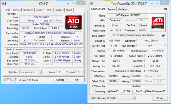
AMD A8-5600K
Pattern is evident from its name, A8-5600K
is a weaker variant of the APU Trinity. The difference between the A8 and A10
series is that two out of the graphics core’s six SIMD engines are turned off
in the A8. As a result, the A8-5600K provides the Radeon HD 7560D graphics core
with 256 stream processors at 759 MHz. The A8's x86 core has no difference
with the core of its senior brother. They are based on two dual-core Piledriver
modules with 2MB of L2 cache per each module. The A8-5600K isn’t much different
from its cousins in clock rates. Its base clock rate is 3.6Ghz that can be
pushed up to 3.9 GHz.
AMD
A8-5600K
In everyday applications the A8-5600K
mostly worked at 3.8GHz but the clock rate is lowered to 3.2GHz at high loads.
Although the A8-5600K is closer to the A10-5700 rather than to the A10-5800K in
its clock rates, its TDP is as high as 100 watts. It may have something to do
with the APU’s overclocking capabilities. Being a K series model, it can be
overclocked by changing frequency multipliers.
A8-5600K’s specs
·
Number of cores: 4
·
CPU frequency: 3.6GHz Base, 3.9 GHz Turbo
·
L2 cache: 4MB
·
Integrated graphics: HD7560D
·
Shader cores: 256
·
GPU frequency: 760MHz
·
TDP: 100W
·
Maximum memory frequency: DDR3-1866